1. Input characteristic: It is the curve between base current I
B and base-emitter voltage V
BE at constant collector-emitter voltage V
CE.
- The input characteristics of a CE connection can be determined by the circuit shown in Fig. 4.29. Keeping V
CE constant (say at 10V), note the base current I
B for various values of V
BE. Then plot the readings obtained on the graph, taking I
B along yaxis and V
BE along x-axis. This gives the input characteristic at V
CE = 10V as shown in Fig. 4.30. Following a similar procedure, a family of input characteristics can be drawn. The following points may be noted from the characteristics:
(i) The characteristic resembles that of a forward biased diode curve. This is expected since the base- emitter section of transistor is a diode and it is forward biased.
(ii) As compared to CB arrangement, I
B increases less rapidly with V
BE. Therefore, input resistance of a CE circuit is higher than that of CB circuit.
Input resistance. It is the ratio of change in base-emitter voltage (Change in V
BE) to the change in base current (Change in I
B) at constant V
CE i.e.
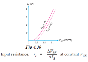
- The value of input resistance for a CE circuit is of the order of a few hundred ohms.
2. Output characteristic: It is the curve between collector current I
C and collector-emitter voltage V
CE at constant base current I
B- The output characteristics of a CE circuit can be drawn with the help of the circuit shown in Fig. 4.29. Keeping the base current I
B fixed at some value say, 5 µA, note the collector current I
C for various values of V
CE. Then plot the readings on a graph, taking I
C along y-axis and V
CE along x-axis.
- This gives the output characteristic at I
B = 5 µA as shown in Fig. 4.31 (i). The test can be repeated for I
B = 10 µA to obtain the new output characteristic as shown in Fig. 4.31 (ii). Following similar procedure, a family of output characteristics can be drawn as shown in Fig. 4.31 (iii).
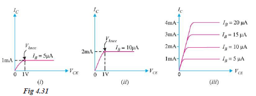
- The following points may be noted from the characteristics:
(i) The collector current I
C varies with V
CE for V
CE between 0 and 1V only. After this, collector current becomes almost constant and independent of V
CE. This value of V
CE upto which collector current I
C changes with V
CE is called the knee voltage (Vknee). The transistors are always operated in the region above knee voltage.
(ii) Above knee voltage, I
C is almost constant. However, a small increase in I
C with increasing V
CE is caused by the collector depletion layer getting wider and capturing a few more majority carriers before electron-hole combinations occur in the base area.
(iii) For any value of V
CE above knee voltage, the collector current I
C is approximately equal to ß × I
B.
- Output resistance. It is the ratio of change in collector-emitter voltage (change in V
CE) to the change in collector current (change in I
C) at constant I
B i.e.
- It may be noted that whereas the output characteristics of CB circuit are horizontal, they have noticeable slope for the CE circuit. Therefore, the output resistance of a CE circuit is less than that of CB circuit. Its value is of the order of 50 kilo-ohms.
jim items answered the question on
November 16, 2018 at 18:10