-
A common base transistor amplifier has an input resistance of 20 ohms and output resistance of 100 kilo-ohms.
(Solved)
A common base transistor amplifier has an input resistance of 20 ohms and output resistance of 100 kilo-ohms. The collector load is 1 kilo-ohm. If a signal of 500 mV is applied between emitter and base, find the voltage amplification. Assume aac to be nearly one
Date posted:
August 14, 2019
.
Answers (1)
-
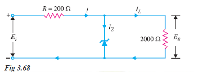
Over what range of input voltage will the Zener circuit shown in Fig. 3.68 maintain 30 V across 2000 O load, assuming that series resistance...
(Solved)
Over what range of input voltage will the Zener circuit shown in Fig. 3.68 maintain 30 V across 2000 Ω load, assuming that series resistance R = 200 Ω and Zener current rating is 25 mA ?
Date posted:
August 14, 2019
.
Answers (1)
-
What value of series resistance is required when three 10-watt, 10-volt, 1000 mA Zener diodes are connected in series to obtain a 30-volt regulated output...
(Solved)
What value of series resistance is required when three 10-watt, 10-volt, 1000 mA Zener diodes are connected in series to obtain a 30-volt regulated output from a 45 volt d.c. power source ?
Date posted:
August 14, 2019
.
Answers (1)
-
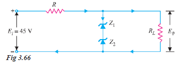
The circuit of Fig. 3.66 uses two Zener diodes, each rated at 15 V, 200 mA.
(Solved)
The circuit of Fig. 3.66 uses two Zener diodes, each rated at 15 V, 200 mA. If the circuit is connected to a 45-volt unregulated supply, determine:
(i) The regulated output voltage
(ii) The value of series resistance R
Date posted:
August 14, 2019
.
Answers (1)
-
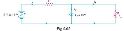
A 10-V Zener diode is used to regulate the voltage across a variable load resistor [See fig. 3.65].
(Solved)
A 10-V Zener diode is used to regulate the voltage across a variable load resistor [See fig. 3.65]. The input voltage varies between 13 V and 16 V and the load current varies between 10 mA and 85 mA. The minimum Zener current is 15 mA. Calculate the value of series resistance R.
Date posted:
August 14, 2019
.
Answers (1)
-
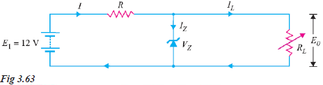
A 7.2 V Zener is used in the circuit shown in Fig. 3.63 and the load current is to vary from 12 to 100 mA.
(Solved)
A 7.2 V Zener is used in the circuit shown in Fig. 3.63 and the load current is to vary from 12 to 100 mA. Find the value of series resistance R to maintain a voltage of 7.2 V across the load. The input voltage is constant at 12V and the minimum Zener current is 10 mA.
Date posted:
August 14, 2019
.
Answers (1)
-
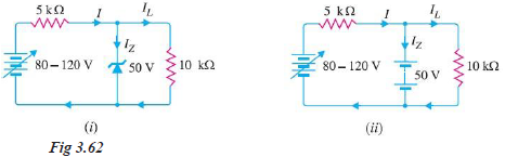
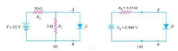
For the circuit shown in Fig. 3.62 (i), find the maximum and minimum values of Zener diode current.
(Solved)
For the circuit shown in Fig. 3.62 (i), find the maximum and minimum values of Zener diode current.
Date posted:
August 14, 2019
.
Answers (1)
-
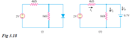
Determine the state of diode for the circuit shown in Fig. 3.18 (i) and find ID and VD. Assume simplified model for the diode.
(Solved)
Determine the state of diode for the circuit shown in Fig. 3.18 (i) and find ID and VD. Assume simplified model for the diode.
Date posted:
August 14, 2019
.
Answers (1)
-
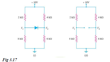
Determine if the diode (ideal) in Fig. 3.17 (i) is forward biased or reverse biased.
(Solved)
Determine if the diode (ideal) in Fig. 3.17 (i) is forward biased or reverse biased.
Date posted:
August 14, 2019
.
Answers (1)
-
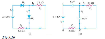
Determine the currents I1, I2 and I3 for the network shown in Fig. 3.16
(Solved)
Determine the currents I1, I2 and I3 for the network shown in Fig. 3.16(i). Use simplified model for the diodes.
Date posted:
August 14, 2019
.
Answers (1)
-
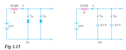
Determine current through each diode in the circuit shown in Fig. 3.15
(Solved)
Determine current through each diode in the circuit shown in Fig. 3.15 (i). Use simplified model. Assume diodes to be similar.
Date posted:
August 14, 2019
.
Answers (1)
-
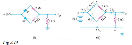
Find VQ and ID in the network shown in Fig. 3.14 (i). Use simplified model
(Solved)
Find VQ and ID in the network shown in Fig. 3.14 (i). Use simplified model
Date posted:
August 14, 2019
.
Answers (1)
-
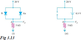
Find the voltage VA in the circuit shown in Fig. 3.13 (i). Use simplified model.
(Solved)
Find the voltage VA in the circuit shown in Fig. 3.13 (i). Use simplified model.
Date posted:
August 14, 2019
.
Answers (1)
-
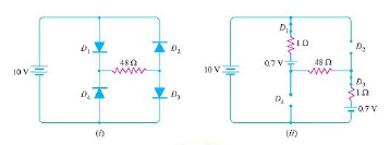
Calculate the current through 48 O resistor in the circuit shown in Fig. below
(Solved)
Calculate the current through 48 Ω resistor in the circuit shown in Fig. below
(i). Assume the diodes to be of silicon and forward resistance of each diode is 1 Ω.
Date posted:
August 14, 2019
.
Answers (1)
-
Find the current through the diode in the circuit shown in Fig. 3.10
(Solved)
Find the current through the diode in the circuit shown in Fig. 3.10
(i). Assume the diode to be ideal.
Date posted:
August 14, 2019
.
Answers (1)
-
An a.c. voltage of peak value 20 V is connected in series with a silicon diode and load resistance of 500 O.
(Solved)
An a.c. voltage of peak value 20 V is connected in series with a silicon diode and load resistance of 500 Ω. If the forward resistance of diode is 10 Ω, find:
(i) peak current through diode
(ii) peak output voltage. What will be these values if the diode is assumed to be ideal ?
Date posted:
August 14, 2019
.
Answers (1)
-
What is the Equivalent Circuit of Crystal Diode?
(Solved)
What is the Equivalent Circuit of Crystal Diode?
Date posted:
August 14, 2019
.
Answers (1)
-
Discuss on Resistance of Crystal Diode
(Solved)
Discuss on Resistance of Crystal Diode
Date posted:
August 14, 2019
.
Answers (1)
-
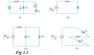
In each diode circuit of Fig. 3.4, find whether the diodes are forward or reverse biased.
(Solved)
In each diode circuit of Fig. 3.4, find whether the diodes are forward or reverse biased.
Date posted:
August 14, 2019
.
Answers (1)
-
How is a Crystal Diode a Rectifier?
(Solved)
How is a Crystal Diode a Rectifier?
Date posted:
August 14, 2019
.
Answers (1)