- It is important to note that a transistor can accomplish faithful amplification only if proper associated circuitry is used with it. Fig. 5.3 shows a practical single stage transistor amplifier. The various circuit elements and their functions are described below:
(i)
Biasing circuit: The resistances R
1, R
2 and R
E form the biasing and stabilisation circuit.
- The biasing circuit must establish a proper operating point otherwise a part of the negative half-cycle of the signal may be cut off in the output.
(ii)
Input capacitor Cin: An electrolytic capacitor C
in (˜ 10 µF ) is used to couple the signal to the base of the transistor. If it is not used, the signal source resistance will come across R
2 and thus change the bias. The capacitor C
in allows only a.c. signal to flow but isolates the signal source from R
5.
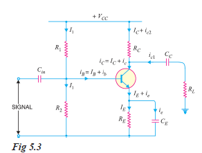
i. Emitter bypass capacitor C
E. An emitter bypass capacitor C
E ( ˜ 100µF ) is used in parallel with R
E to provide a low reactance path to the amplified a.c. signal. If it is not used, then amplified a.c. signal flowing through R
E will cause a voltage drop across it, thereby reducing the output voltage.
ii. Coupling capacitor C
C. The coupling capacitor C
C (˜10µF) couples one stage of amplification to the next stage. If it is not used, the bias conditions of the next stage will be drastically changed due to the shunting effect of R
C. This is because R
C will come in parallel with the upper resistance R
1 of the biasing network of the next stage, thereby altering the biasing conditions of the latter. In short, the coupling capacitor C
C isolates the d.c. of one stage from the next stage, but allows the passage of a.c. signal.
- It may be noted that a capacitor offers infinite reactance to d.c. and blocks it completely whereas it allows a.c. to pass through it.
-
Various circuit currents: It is useful to mention the various currents in the complete amplifier circuit. These are shown in the circuit of Fig. 5.3
(i) Base current. When no signal is applied in the base circuit, d.c. base current I
B flows due to biasing circuit. When a.c. signal is applied, a.c. base current i
b also flows. Therefore, with the application of signal, total base current i
B is given by:
i
B = I
B + i
b(ii) Collector current. When no signal is applied, a d.c. collector current I
C flows due to biasing circuit. When a.c. signal is applied, a.c. collector current i
c also flows. Therefore, the total collector current i
C is given by:
i
C = I
C + i
c where I
C = ß I
B = zero signal collector current i
c = ß i
b = collector current due to signal.
(iii) Emitter current. When no signal is applied, a d.c. emitter current I
E flows. With the application of signal, total emitter current iE is given by:
i
E = I
E + i
eIt is useful to keep in mind that:
I
E = I
B + I
Ci
e = i
b + i
cNow base current is usually very small, therefore, as a reasonable approximation,
I
E ˜ I
C and i
e ˜ i
c
Wilfykil answered the question on
August 15, 2019 at 08:32